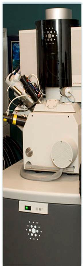
FEI Helios NanoLab Dual-beam
· Scanning Electron Microscopy – 1.5 nm resolution
· BSE microscopy (dedicated VCD detector)
· STEM
· Focused Ion Beam milling
· AutoSlice and View™ – automated sequential mill and view to collect series of slice images for 3D reconstruction.
· Conductor (Pt) and Insulator (SiO2) deposition
· Cryo-Microscopy and Cryo-Ion milling (Quorum)
· E-Beam Lithography (Nabity)
· EDS spectrum and mapping (Edax TEAM)
· 3-D reconstruction (Amira)
· NanoBuilder™ allows patterning of large and complex nanostructures accurately on multiple sites, supporting all DualBeam™ patterning processes: focused ion beam (FIB) milling, gas-assisted FIB milling, FIB induced deposition, and electron-induced deposition. Patterning of all layers is executed fully automatically.